Design of a Custom Direct Memory Access Module and Its Implementation in a System-on-Chip
Project Partners
- Client Organization: Procenne – Güvenpark Bilişim Teknolojileri Ar-Ge Tic. Ltd. Şti.
- Executing Organization: Istanbul Technical University, Embedded Systems Design Laboratory
- Funding Organization: TÜBİTAK 1505 University–Industry Cooperation Support Program



Project Team
- Project Leader: Prof. Dr. Berna Örs Yalçın
Project Overview
Hardware security modules (HSMs) enable cryptographic algorithms to be implemented securely in hardware while providing high performance.
Security protocols that perform critical functions in fields such as finance, defense, intelligence, and healthcare often process large blocks of data. Executing these protocols at high speed can be achieved through the use of algorithm-specific hardware accelerators.
Dedicated hardware units implemented on ASICs or FPGAs for cryptographic algorithms operate much faster than software implementations. However, a processor is still required for system control and communication with external systems. Algorithm-specific hardware units are connected to this processor to form a system-on-chip.
The input and output data of cryptographic algorithms may be between 4 and 128 times wider than the data-bus widths of contemporary processors. When algorithm-specific hardware units are connected directly to the processor, a significant portion of the system execution time is spent transferring data, reducing overall system efficiency.
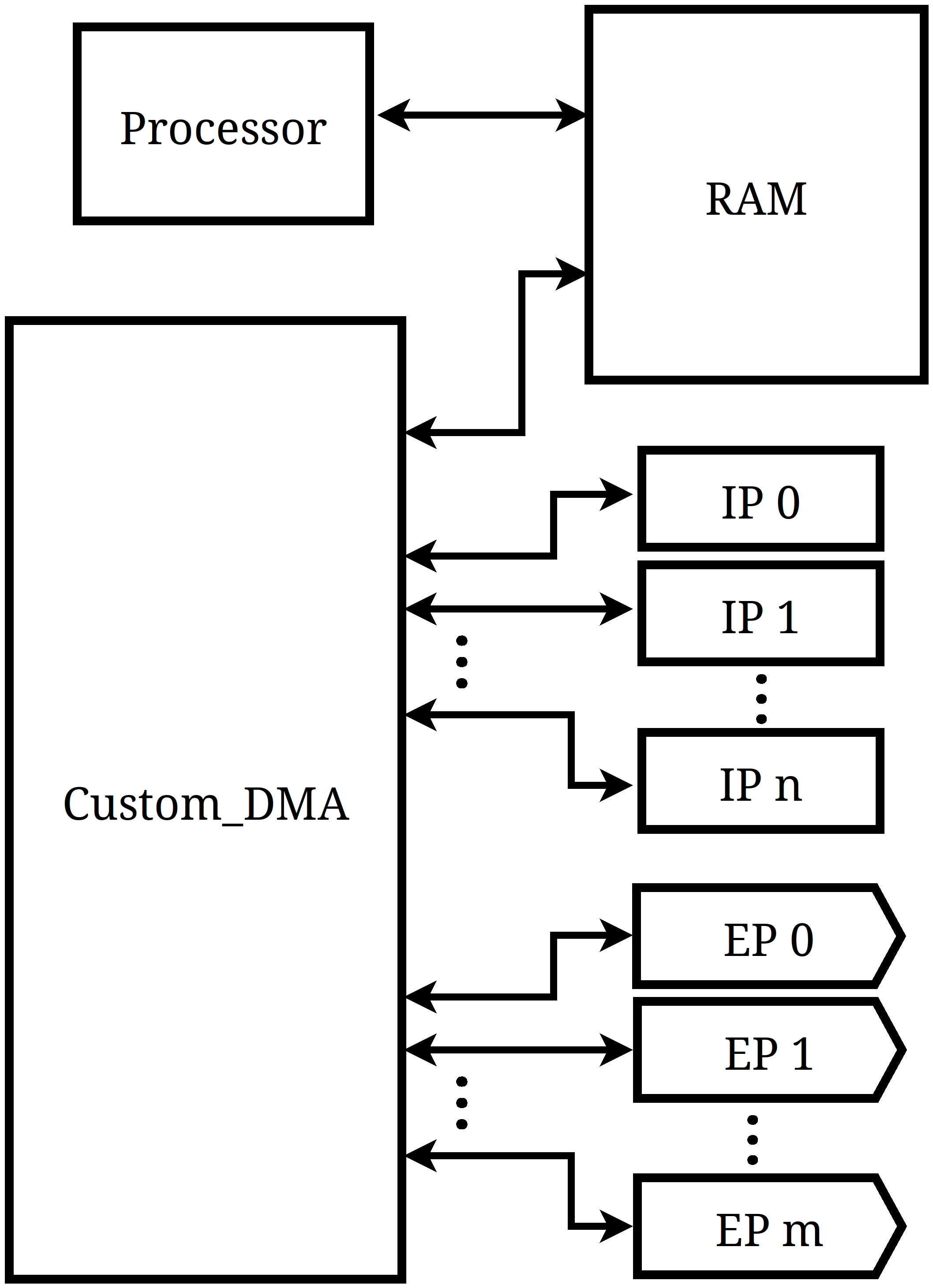
In this project, a custom direct memory access module will be designed to transfer commands and data among interfaces such as PCIe, algorithm-specific hardware units, and the processor through the RAM interface of a RISC-V processor.
Using the designed module, a high-speed HSM will be implemented as an FPGA-based system-on-chip. After functional testing, performance evaluation, and detailed verification have been completed, the system will be designed, fabricated, and tested as an ASIC.
Methodology
During the design of the custom direct memory access module, existing custom DMA architectures will be examined, and solutions applied to similar problems in the literature will be investigated.
Following the literature review, an architecture that provides the required behavior and incorporates new performance-enhancing features will be finalized. Particular attention will be paid to ensuring that the design is flexible, extensible, easy to implement, and practical to use.
The system-on-chip, consisting of a processor, algorithm-specific hardware units, and memory, will be designed to minimize performance losses caused by data communication.
The system is planned to include external interfaces such as Ethernet, UART, and PCIe for communication with external devices. Communication between these interfaces and memory will be managed by the custom direct memory access block designed within the project. This approach will prevent external communication from creating additional processing overhead on the processor.
System-on-Chip Design
- A system-on-chip will be designed using a Zynq processor, a direct memory access block, cryptographic cores, and a PCIe interface.
- Tests covering all data-transfer operations will be prepared, and behavioral simulations will be performed using test files.
- The system will be implemented according to the performance requirements identified during the analysis phase and then programmed onto an FPGA.
- Test software will be developed to measure memory-access speeds on the FPGA and determine whether the performance constraints are satisfied.
Custom Direct Memory Access Design
- A system diagram showing the RISC-V processor, cryptographic cores, PCIe interface, and BRAM interfaces will be prepared.
- The functional behavior required from the system will be defined.
- Input and output interfaces that can support the target communication speed will be evaluated.
- A block architecture that satisfies the required speed while using the minimum possible hardware resources will be selected.
Design of a System-on-Chip Communicating Through the Custom Direct Memory Access Module
- An open-source RISC-V processor suitable in terms of performance and area utilization will be selected.
- IP blocks capable of communicating with the existing interfaces of the RISC-V processor will be developed.
- The block-level architecture of the system-on-chip will be created.
- The required drivers for the custom direct memory access module will be developed.
- The VHDL implementation of the system will be produced.
- Behavioral simulation, synthesis, implementation, and post-synthesis simulation will be performed.
- After simulation and verification have been completed, the FPGA programming file, or bitstream, will be generated and programmed onto the FPGA.
Functional Verification and Performance Testing
- Test vectors will be generated for system verification.
- Test data will be transmitted from a computer to the FPGA using a communication protocol.
- Responses received from the FPGA will be read by the computer and compared with the expected results.
- If an error is detected, its cause will be investigated, the issue will be corrected, and the tests will be repeated.
- Separate test files will be prepared for performance testing, and performance results will be measured for each system operation.
ASIC Implementation
After functional and performance verification has been completed, the system-on-chip will be implemented and fabricated as an ASIC and tested on a specially designed printed circuit board.